4
Dec
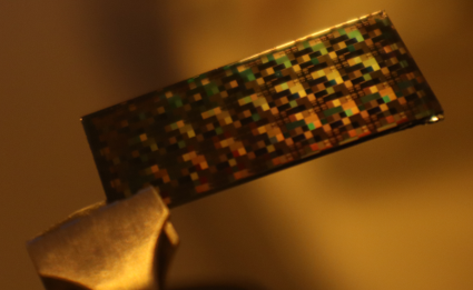
We are excited to announce a new domestic class 100 R&D facility for semiconductor device prototyping located in Geneva, NY. This lab continues to expand our team's offerings and project potential for our partners. Complete with a comprehensive toolset for the fabrication and packaging of sub-micron devices.
We are seeking to help bridge the gap from lap to fab, where we specialize in developing process solutions for all forms of devices. Large foundries are often cost prohibitive for early ventures, while universities represent a beaucratic headache and IP concerns. NanoTech strategies can be your domestic partner to help fill in the gaps and scale.