Process flow design from concept to test vehicle

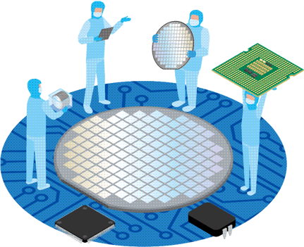
We built our Class 100 cleanroom to deliver fast, repeatable device prototypes.
In-house capability highlights:
Process flow design from concept to test vehicle
~0.75um features with options for smaller isolated features
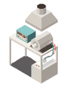
Core steps executed internally, with growth and packaging partners as needed
Experience across Si, GaN, SiC, Ga2O3, and related stacks

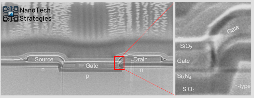
Initial device modeling is critical to virtually "build" your device and peer into the inner workings of the device to explore its functionality. We can assist in building device simulations to help you gain further insight.
When you are set with a device, layout can be a critical aspect to ensure it matches with the manufacturing process to achieve success device results. We can work with you to help develop your mask designs for your complete process flow.
These capabilities support rapid learning loops during prototyping. We can surface root causes and validate device behavior without slowing the schedule.
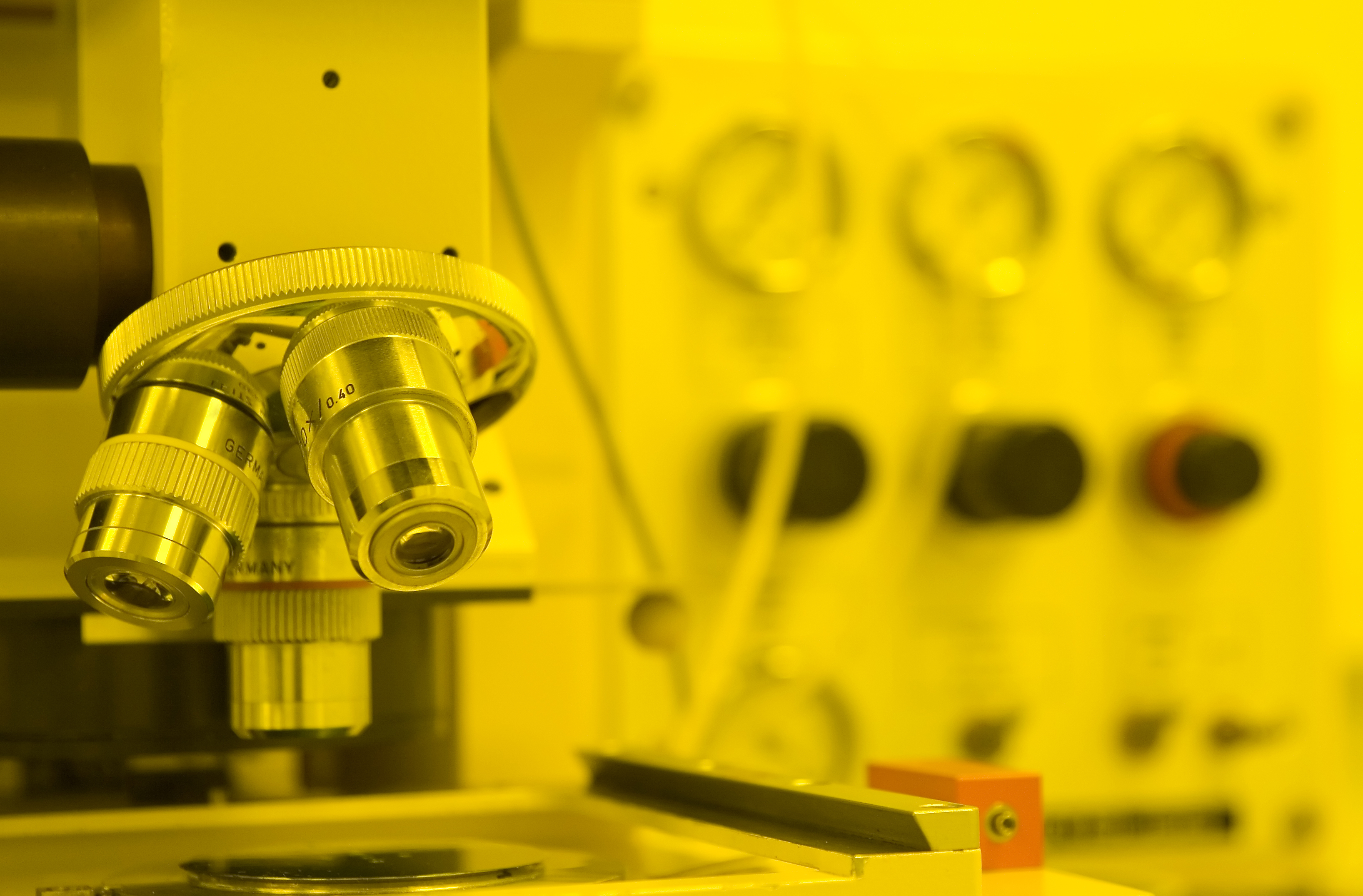
Device-level inspection to isolate yield or performance issues early in the flow.
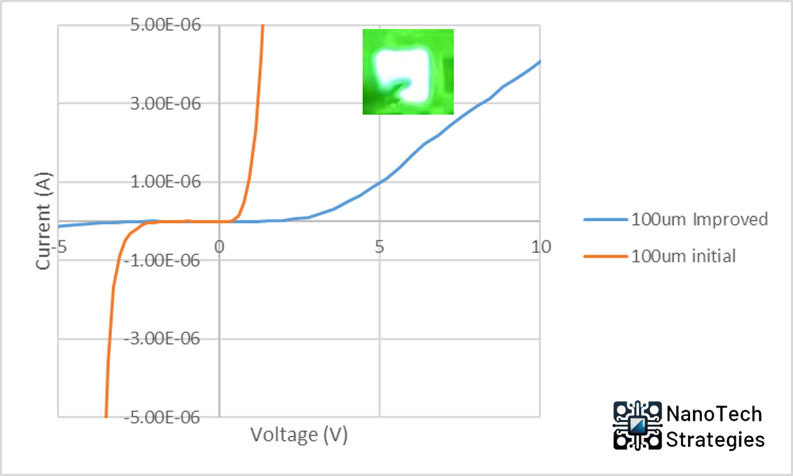
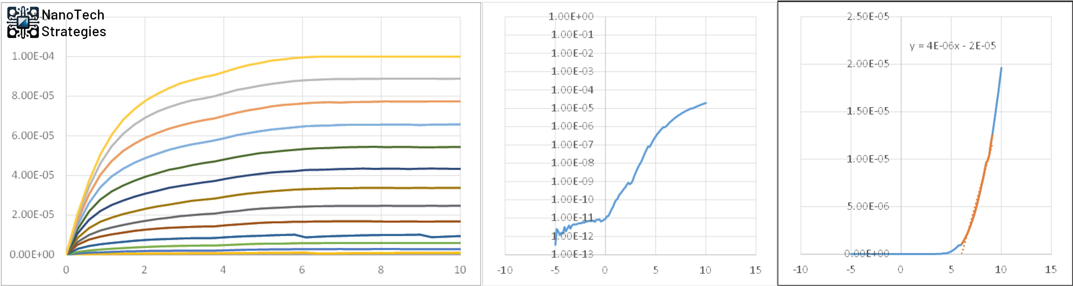
Electrical and optical characterization to validate models and device performance.
Clean datasets ready for reporting and stakeholder review.
We are a US company based in Geneva, NY with the flexibility and focus to move quickly without sacrificing rigor.
Flexibility in project size
Wide range of materials and capabilities
Experienced tackling problems
Detailed communications and insight